Welcome back to the third and final post in this series about building circuit designs in Alteryx, where I'll discuss the design challenges of building up an Arithmetic Logic Unit (ALU) into a Central Processing Unit (CPU). In case you need to catch up, the previous posts can be found here:
Computing Digital Logic and Building Circuits in Alteryx Designer - (1/3) Digital Logic
Computing Digital Logic and Building Circuits in Alteryx Designer - (2/3) ALU Design
When we last left off, we had designed a functioning ALU, but were in a real cliffhanger with the CPU design:
 Each red error indicates an invalid dependency of flow. (The instruction decoder design is expanded inside a Tool Container, as it has too many outputs to work well as a macro.)
In this last post, I'll explain how I got myself into this situation, and explain some of the design considerations involved with introducing memory to the circuit design.
A Quick Crash Course On Memory
One of the fundamental building blocks for augmenting an ALU into a full CPU is the ability to store data.
To this end, I wanted to emulate something like a D-Flip-Flop, which delays any input by 1 time-step:
input ||0111010111...
output||0011101011...
... and to then use that component in a design called a Register, which loads an input value into memory if the load flag is set, and otherwise outputs its currently remembered value:
input |011001000000...
load  |001000001000...
======================
output|000111111000...
Such registers can be combined to form Random Access Memory (RAM), where data can be read from or written to specific addresses in the RAM.
Registers also play a part in storing the previous values of a Counter component, which increment its count value over time.
And a Counter is instrumental in tracking which stored instruction to execute next, and so on...
Stumbling Block: Sending Outputs To Future Cycles
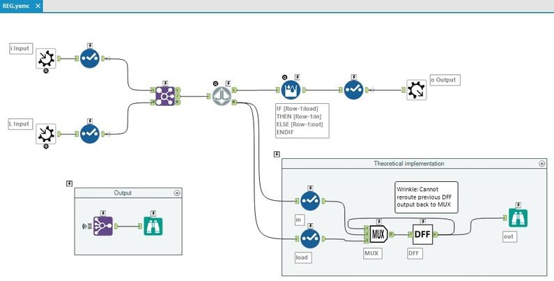
When exploring the possibility of expanding the ALU into a CPU, the persistent question was how to deal with non-linear flow of data. For instance, a register can be designed with MUX and D-Flip-Flop components, but the output of DFF feeding into the first input of MUX would be an unresolved dependency relationship:

Using a Multi-Row Formula could work as a quick patch for the register macro, but that limitation with data flow continued to be an issue when building up the physical CPU map. Revisiting the first image of this post, the below is a valid CPU circuit design, but fails to run in Alteryx:
 Each red error indicates an invalid dependency of flow. (The instruction decoder design is expanded inside a Tool Container, as it has too many outputs to work well as a macro.)
I suppose a workaround for such limitations could be implemented with an Iterative Macro. But such a macro-based design was unappealing, as it would have been nice if the layout of the CPU macro could match a potential physical wiring configuration.
The funny thing is that Alteryx was still incredibly helpful for implementing the HDL code for another simulator environment. By gradually deleting each tool from the canvas as I translated the corresponding HDL lines, I was able to accurately transcribe my Alteryx design with little frustration.
Future Work: Constructing More Operations Through Software, Without Needing More Hardware
When a CPU is constructed from an ALU wired with registers, counter and other memory components, the results of various instruction sequences can be saved. This allows for the creation of other arithmetic constructs (such as multiplication or division from addition or subtraction), or the recreation of boolean logic from a series of NAND operations.
For example, how would we support subtraction of numbers? To calculate A - B:
- To get the negative value of B, push B into Input 1 with the bitwise negate enabled. ADD that with 1.
- Save the result of -B in memory
- Load A and -B into the inputs for ADD
Operations like multiplication and division, as well as the handling of decimal numbers, are typically handled by a dedicated coprocessor. But replicating them with instructions is theoretically empowering, as hardware is typically harder to change than software.
Closing Remarks
That sums up some of the loose ends left with integrating the ALU into a CPU design. Any questions about the topics introduced here? How about any ideas about what could be done differently? Feel free to comment below.