
When I first saw an Alteryx workflow, the canvas of connected tools reminded me of logic gate circuit diagrams:
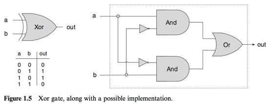
Xor gate example design from The Elements of Computing Systems
These diagrams are a key exercise in the design of an Arithmetic Logic Unit (ALU), a circuit component that can compute a small-but-powerful collection of arithmetic operations. You may recognize some of these operations including addition, subtraction, and boolean comparisons. Astonishingly, one particular boolean operator can serve as the fundamental building block of this entire ALU system.
This building block is called the “NAND” gate (a circuit that indicates through its output signal, if two input signals are both not “on”). The boolean logic of NAND can be summarized with the following table:
| Input 1 | Input 2 | Output |
| false | false | true |
| false | true | true |
| true | false | true |
| true | true | false |
When one can construct a NAND gate, its copies can be reused to build greater abstractions, such as other boolean operations (AND, NOT, OR, XOR). I wanted to test if such a system was possible to implement in Alteryx, following the tradition of building ALUs and CPUs in software environments not intended to simulate computing hardware. (On this subject of arithmetic circuit design, The Elements of Computing Systems is a fantastic resource!)
Given that there was precedent for Alteryx simulating other computation devices, such as @chris_love's Enigma Machine, I once asked @GarySchwartz if anyone had ever used Alteryx to design circuits. Gary mentioned that perhaps such designs could be accomplished with custom macros, but he couldn't think of any examples at the time. In the spirit of doing anything in Alteryx, challenge accepted!
Innovation Days and Book Club at Alteryx
The opportunity to prototype this idea came with our quarterly Innovation Days, where Alteryx employees are given two days to work on any project that they would like. Examples of such projects include Neil's creation of a tool with Javascript and HTML, as well as my implementing the Add to New (Tool) Container functionality requested in the ideas forum.
Combined with additional practice from our internal Alteryx Book Clubs (where we learn how to use Alteryx by solving the same exercises shared on the community), I felt that I had the tools and the time to make this project a reality. Thus I embarked on a project to simulate an ALU in Alteryx!
Comparison With Traditional Hand-Diagrammed Designs
The most commonly recommended approach for designing an ALU is to draw out a diagram by hand, and then calculate the effect of each component on the overall design:
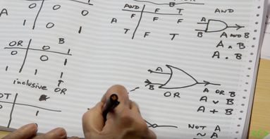
AND OR NOT - Logic Gates Explained - Computerphile
Such designs are then hand-translated into text-based Hardware Description Language (HDL), which is code that describes your circuit design to a simulator:
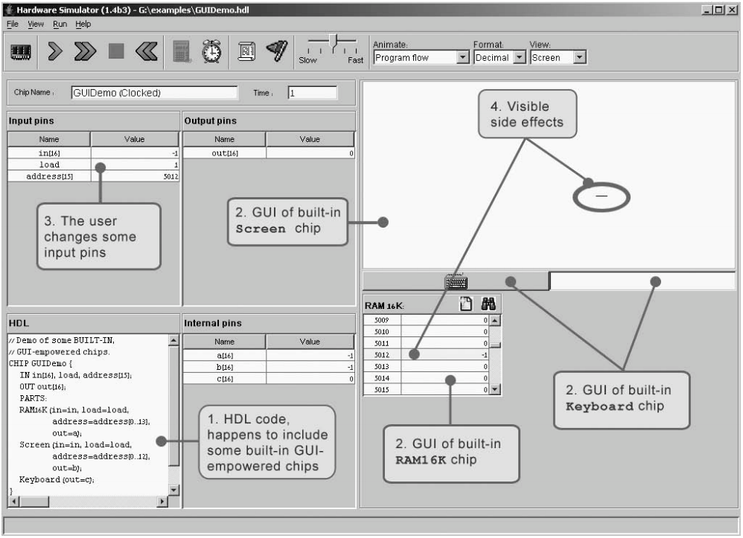
Hardware Simulator for The Elements of Computing Systems exercises
(... where you don't even get the luxury of editing the text inside the HDL window. You have to modify the text file in an editor and reload the solution!)
It seemed that Alteryx had potential for greatly simplifying this design process. A drag and drop interface would be much easier to visualize and compose in, compared to writing HDL code. And Designer's Browse-Everywhere functionality would be a faster, more accurate way to calculate the effect of each node on the design, without having to manually update a paper diagram.
Hello NAND!
To begin working with NAND gates, we first need a way to create them. NAND gates can be built with various designs, either through circuitry or with redstone mined from the lands of Minecraft. In this case, we'll create a macro that simulates a NAND gate in Alteryx.
First of all, how would we represent the values of a high or low signal in the circuit? Revisiting the earlier boolean logic table of NAND, the inputs and outputs can be represented with the famous 1's and 0's of computer code:
| Input 1 | Input 2 | Output |
| 0 | 0 | 1 |
| 0 | 1 | 1 |
| 1 | 0 | 1 |
| 1 | 1 | 0 |
For the rest of these posts, I'll be using the numbers 0 and 1 to indicate a "low" and "high" signal respectively. This is akin to saying that a switch is "off" (0) and then "on" (1). Or in the case of a boolean logic representation, we're saying that a result is "false" (0) or "true" (1).
So for our NAND macro, if both inputs A and B are true (i.e. 1), the result should be 0, while any other configuration would output a 1. Such logic can be easily represented with a single Formula tool:
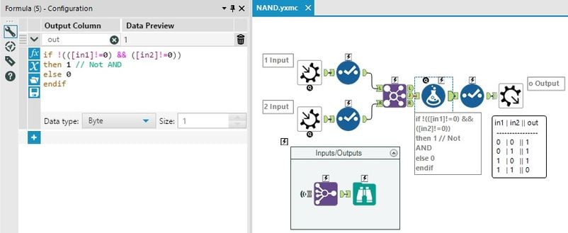
Building Additional Boolean Primitives from NAND
Now that we have a NAND component ready, the next step is to build the other boolean operations.
Step 1: Boolean NOT
Given that the inputs into a NAND gate could be a high (1) or low (0) signal, how could another boolean operation be constructed?
What if one of the two NAND inputs was always true?
| Input 1 | Input 2
(Always 1) | Output |
| 0 | 1 | 1 |
| 1 | 1 | 0 |
... and ignoring the always true input, how does the remaining input relate to the output?
... it looks like the input got reversed! That result matches the logic table of the NOT operation, which flips the bit of a single input. To put it another way, a NOT gate is a NAND gate that takes only one input, and that input is compared unconditionally to a high signal (on).
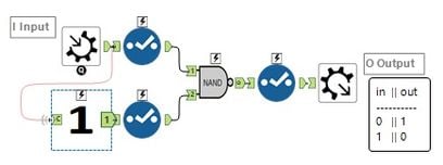
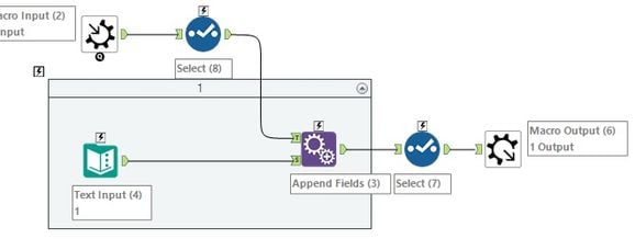
But for each record field that flows into the first input anchor of NAND, how do we emit a corresponding high (1) value to the second anchor? Easy, let's use an Append Fields tool on the input!
Step 2: Boolean AND
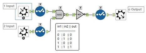
Now that we can get the NOT of a "Not-AND" NAND, we can compute AND:
Step 3: Boolean OR
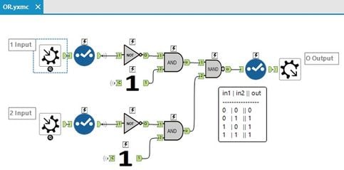
Boolean OR differs a little from the usual understanding of A "or" B. If either A or B is true, then OR is true:
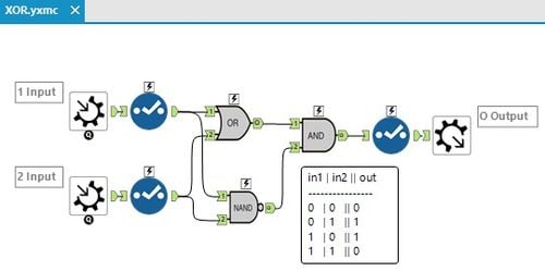
Step 4: Boolean XOR
Meanwhile, XOR conforms more to the conventional meaning of choosing between A "or" B, but not both:
What Boolean Operations Have We Created?
Let's recap what we have so far:
- A NAND gate that compares 2 inputs, and returns true if and only if both inputs are NOT both true.
- A NOT gate that inverts a single input, where true turns to false, and false turns to true.
- A AND gate that takes 2 inputs and returns true only if both inputs are true.
- An OR gate that takes 2 inputs and returns true if either input is true.
- An XOR gate that takes 2 inputs and returns true if only 1 of the inputs is true.
Comparison: Alteryx Versus HDL Simulators
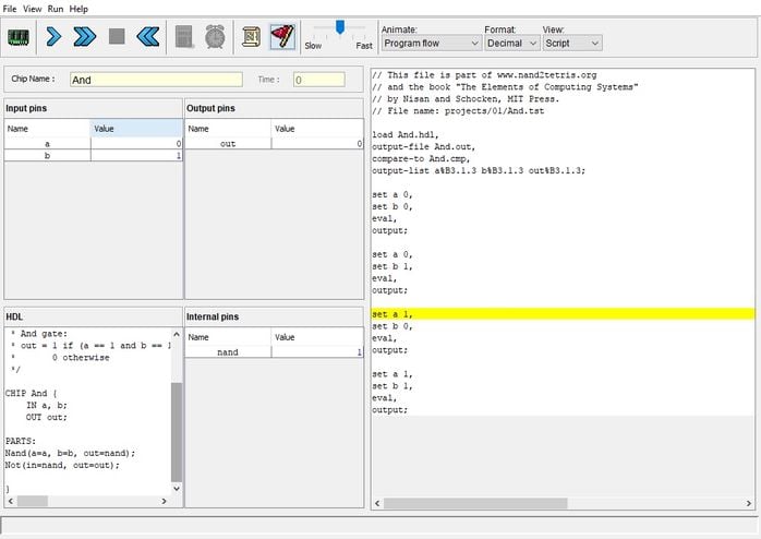
In contrast with Alteryx's drag and drop approach, the NAND To Tetris software environment involves translating a design into HDL code:
CHIP And {
// 0. External API for AND chip
	IN a, b;
	OUT out;

// 1. component list and
// 2. component wirings
	PARTS:
	Nand(a=a, b=b, out=nand);
	Not(in=nand, out=out);
}Not exactly quick to visualize right?
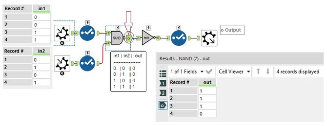
In addition, Alteryx's Browse-Everywhere functionality was a huge help for debugging more convoluted designs in later macros, as I could click on the output for any macro design and view the results of sample inputs:
Compare this one-click introspection against the debugging interface of an HDL simulator:
Conclusion Before The Break
When specifying the design of circuits, the usual custom is to draw designs out on paper, before hand-translating them into HDL language. But why limit oneself to paper and code when you can use Alteryx? Without the need to refer to HDL language specs, Alteryx provided a canvas where results are instantly evaluated with a single click. And with the Browse-Everywhere functionality of each workflow anchor, it was simple to observe the effects of each individual boolean operation.
But with all that said and done, how will deriving all those boolean operators in Alteryx lead to something like numeric addition? Join me next time as we combine the elements created thus far into a working ALU design!
Up Next:
Computing Digital Logic and Building Circuits in Alteryx Designer - (2/3) ALU Design