
Welcome to part 2 of this series on an Alteryx-powered circuit design, where we'll combine what we've learned so far to create an Arithmetic Logic Unit (ALU) in Alteryx Designer! To catch up, the first article can be found here.
Previously, we had created the ingredients of various boolean operations, such as AND, XOR, OR, NOT, and of course NAND. In an ALU design, large numbers of these operations are pushed through the machine. For such bulk calculations, it would be convenient to describe them with a concise representational notation. Enter the idea of a bus...
Representing Multi-Bit Operations With Buses
The core idea of a "bus" is that if we want to process 1 bit of information, we likely want to perform the same action for a series of 4, 16, or even more bits. And as we collect these multi-bit arrays, we also want to track the order that they are aligned, analogous to how we know that 21 is a larger number than 12 in decimal notation. Such an ordered series of 1's and 0's can be combined into binary numbers, much like how decimal numbers are represented by the ten numbers between 0 through 9.
Proof of Concept: 4-Bit Numbers
For example, we could represent numbers as 4-bit inputs. These would be composed as strings of 1's and 0's, where "0100" would represent 4 bits with the 2nd bit being flipped on.
To streamline the handling of these 4-bit numbers, I created a macro for splitting a string (composed of 4 bits) into the 4 individual bit outputs...
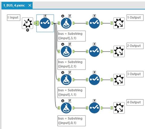
... as well as a complementing macro to combine 4 input bits into their representative output string...
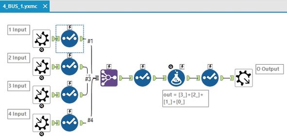
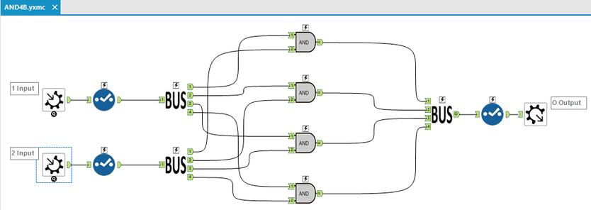
The combination of both macros simplifies the wiring of 4-bit bus versions of each of the boolean chip designs, such as with this 4-bit version of an AND gate:
Expanding to 16-Bit Numbers, and Working With Hexadecimal Inputs
With all that said, any 4-bit number has quite a narrow range with only 4^2 (i.e. 16) possible values. So we'd like to support at least 16-bit numbers with 2^16 (i.e. 65536) possible values.
However, I found it a bit unwieldy to access the anchors of macros defined with 16 inputs or outputs:

So, I took the shortcut of creating a 16 bit NAND macro, where 4 hexadecimal characters from 0-9 and A-F are used to represent the numeric range of 0-15:
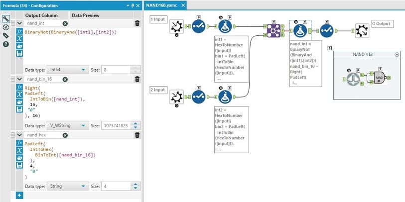
The BinaryNot, BinaryAND, IntToBin, IntToHex, and other Formula functions are part of Alteryx's in-built capabilities for calculating numbers in Hexadecimal and Binary form.
On top of such pre-existing hexadecimal library functions, I added some additional handling of negative numbers represented with 2's-complement notation. Normally such details are hidden by the user-facing side of the computing environment (as integers, floats, doubles, etc), but I wanted to directly display bits of 1's and 0's in a string format. For example, I needed to zero-pad each binary number to 16 bits wide, when less than 16 characters were output by IntToBin. And when IntToBin returned more than 16 characters, I clipped the string to only the rightmost 16 bits.
Implementing Control Flow in Binary Circuits
Changing the behavior of later outputs based on conditional inputs is an important capability in Alteryx. This is also true with our arithmetic circuit, where such conditional logic is implemented using MUX and DEMUX chips.
MUX
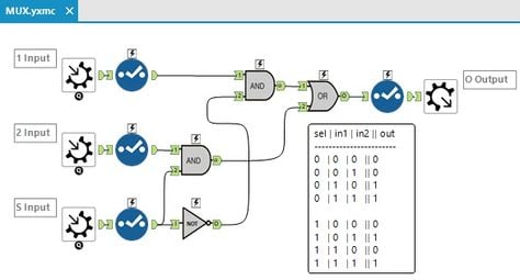
Sometimes it is helpful to take 2 input streams of bits, and to choose which bits to pass downstream with a "select" input.
A corresponding Alteryx Formula would look like:
IF [Select]
THEN [Input2]
ELSE [Input1]
ENDIF
In a similar manner, MUX allows you to choose which of 2 inputs should be passed through to the output flow, based on another selector input.
In the below example:
- The 1st input is selected as the output when the Select input is 0.
- But otherwise the 2nd input is output when Select is 1:
DEMUX
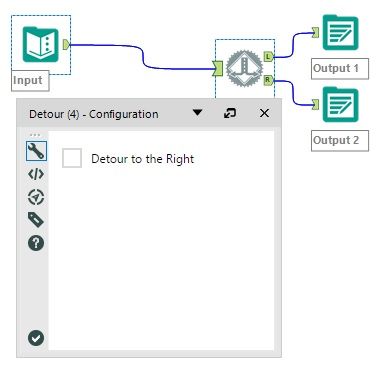
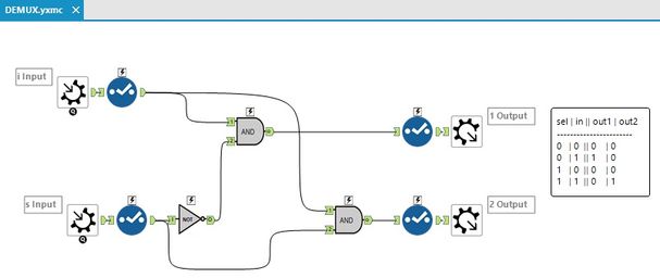
Meanwhile, DEMUX is more analogous to deciding where a train of bits should go, by flipping a "select" switch that decides the output direction among two tracks.
In a way, this operation is akin to records passing through a Detour tool, where the "Detour to the Right" option plays the role of the "select" switch:
Along such lines, DEMUX uses the Select input to decide which exit anchor (output1 or output2) to send the Input data through, while leaving the other exit anchor with a low signal of 0:
1 + 1 = 10: Arithmetic in Binary
Now that we have the basic building blocks of logic, the ability to add 2 numbers would be a rather useful improvement. But before we can add n-bit numbers, we need to be able to add 1-bit numbers in a Half-Adder chip:
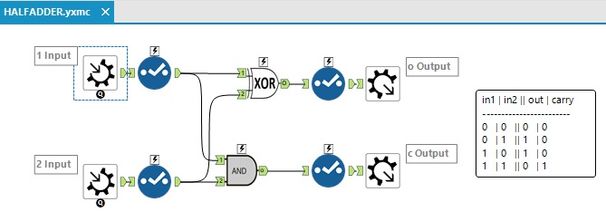
...where the output is split between the addition result, and the carry/remainder of the 1 bit addition.
Half-Adders can then be strung together into a Full-Adder, which can account for the carry results of previous 1-bit additions:

Multi-bit addition can then be accomplished by stringing together N-numbers of Full-Adders, such as with this 4-bit Full-Adder:

This kind of design for the addition of numbers has implications for a number of infamous edge cases in computation, such as integer overflow when addition results exceed the maximum or minimum range of the number type.
Constructing the ALU
With addition and boolean logic implemented, we can now construct an ALU:

The purpose of an ALU is to take 2 inputs, and process them based on the setting of an operation code (opcode). An opcode is like a configuration for your computing machine, where you can specify options such as:
- Whether the 2 inputs are to be fed into an addition operation, or a NAND operation.
- Whether either input should be computed with its own bits flipped. (This is especially useful for handing negations or subtractions.)
- Whether the final output should itself be bitwise flipped
Such options can be represented by 4 opcode bits with the following spec:
opCode[4] -> if 1: negate in1 bitwise
opCode[3] -> if 1: negate in2 bitwise
opCode[2] -> if 0: out = (in1 ADD in2); if 1: out = (in1 NAND in2);
opCode[1] -> if 1: negate out bitwise
A Note on Bitwise vs Numeric Negation
Notice that the earlier opcode spec calls for bitwise negation, where all the bits are flipped for a specified input. The consequences for that distinction are straightforward in the case of NAND bitwise operations, but have surprising implications when working with negative numbers.
For instance, there's a popular trick with getting the arithmetic negative value of binary numbers represented with 2's-complement notation. This is accomplished by first performing a bitwise-NOT on the value, and then adding 1.
Take for example the number 1, or 0000000000000001 in binary. A bitwise negation would result in 1111111111111110 (i.e. -2). Adding 1 would result in 1111111111111111, which is -1 in 2's complement form. I'll leave it as an exercise for the reader to prove that the same procedure works for converting -1 to +1 again.
So what if we add 1 to -1? That would be 0 right? Adding 1 to 1111111111111111 would result in a series of carrys that result in (1)0000000000000000, where the leftmost carry (1) is dropped and the result is 0 in binary. This behavior extends to any combination of 2's-complement numbers, where adding numbers of differing signs results in a output with the correct signage.
Demoing the ALU as an Analytic App
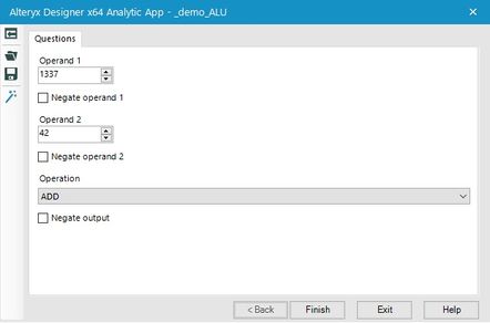
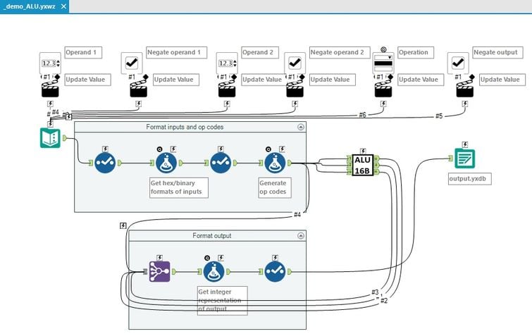
To demo the ALU for Innovation Days, I created an Analytic App that wraps the inputs of the ALU with drop-down menus:

Next Step: A CPU?
With an ALU constructed, the next major enhancement would be to create a Central Processing Unit (CPU), where memory is introduced into the system. With memory, instructions can be stored to create programs, which can be later decoded from their machine code bit format, and finally fed into the ALU. The results of the ALU can then be stored back into memory, which can be reused for future computations. I took some steps toward that direction, and even had a theoretically correct CPU drafted in a workflow, but ran into a wall:
 Each red error indicates an invalid dependency of flow. (The instruction decoder design is expanded inside a Tool Container, as it has too many outputs to work well as a macro.)
So close and yet so far! In the next and final post of this series, I'll go over my stumbling blocks with this CPU implementation, and cover some of the design considerations for introducing memory to the ALU system. But first, let's wrap up what we have so far...
Closing Remarks
As @steveahlgren once wrote, "This is another perfect example of how Alteryx can be used (abused?) to solve nearly any problem, regardless of the domain." And sometimes that domain is computation itself, on the level of bits in the computing machine.
Attached to this post is a zip file containing all the macros used to construct the ALU, as well as the incomplete work for the CPU design.
Hopefully that inspires you to play with the tools you have at your disposal and to expand the range of applications your workflows address. And remember to hold onto The Thrill of Solving (echo echo echo...). Any questions about the design? Have any workflows you would like to share? Feel free to comment below.
Additional Resources